


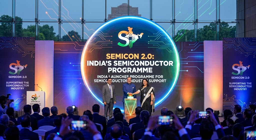
India Launches Semicon 2.0 Programme for Semiconductor Industry Support
The CSR Journal Magazine

The Ministry of Electronics and Information Technology (MeitY) has laid out specific requirements for companies aiming to participate in the newly announced Semicon 2.0 programme. This initiative comes with a framework of investment thresholds, revenue expectations, and technology prerequisites tailored for various segments of the semiconductor value chain.

Criteria for Participation

For firms involved in strategic semiconductor design, they must be incorporated and headquartered in India, alongside demonstrating significant operational and workforce presence within the country. Additionally, ownership and control must rest with Indian citizens. These companies may collaborate with global entities, research institutions, or academic bodies.

Similarly, firms engaged in commercial semiconductor design are required to be incorporated and based in India. Ownership must also be with Indian citizens or Overseas Citizens of India (OCIs).

Funding and Support for Startups and MSMEs

Startups and Micro, Small, and Medium Enterprises (MSMEs) will be eligible for milestone-based seed funding. The funding can cover up to 50 per cent of project costs or a maximum of Rs 15 crore, whichever is lower. Companies supported by venture capital or private equity may also receive equity co-investment as part of this scheme.

Furthermore, larger eligible firms can benefit from royalty financing, whereby they are liable to pay 5 per cent of the net revenue generated from the related product or technology until 1.5 times the governmental support is repaid. For newly developed semiconductor intellectual property (IP), chips, and system-on-chips (SoCs), eligible applicants can receive a 9 per cent reimbursement on net sales over a five-year period, capped at Rs 30 crore for each application and Rs 120 crore for each company.

Investment Requirements for Facilities

The programme outlines strict investment and revenue criteria for various types of facilities. Research and development (R&D) for equipment requires a minimum investment of Rs 300 crore and generates revenue of Rs 120 crore. Facilities producing raw materials need an investment of at least Rs 50 crore and a minimum revenue of Rs 20 crore. Additionally, testing and characterisation facilities necessitate an investment of Rs 100 crore and revenue of Rs 40 crore.

For manufacturing equipment and components, companies must invest at least Rs 300 crore and achieve a revenue of Rs 120 crore. These segments will be eligible for 30 per cent government support on qualifying capital expenditures. Equipment and component manufacturers may also qualify for a production-linked incentive (PLI) of between 10 per cent and 2 per cent related to the value of components sourced from domestic producers for a period extending to FY2028-29, limited to 50 per cent of qualifying capital expenditure.

Specifics for Advanced Manufacturing

Silicon wafer fabrication facilities face the most rigorous criteria, requiring an investment of at least Rs 20,000 crore and a minimum revenue of Rs 7,500 crore over any of the last three financial years. These projects must utilise 300-mm wafers with a capacity of no less than 40,000 wafer starts each month. The government will provide 40 per cent of qualifying capital expenditure on a pari-passu basis for such initiatives.

For compound semiconductors, photonics, and discrete semiconductor fabs, the programme sets a minimum investment threshold of Rs 500 crore and a revenue minimum of Rs 200 crore. These projects will receive 35 per cent support for eligible capital expenditure.

In addition, advanced packaging projects under ATMP/OSAT will require a minimum investment of Rs 1,000 crore, with 35 per cent capex support provided. The same investment and revenue requirements will afford legacy packaging projects 25 per cent support.

Conclusion and Implementation Timeline

The notification regarding Semicon 2.0 follows the Union Cabinet’s approval of a Rs 1.27 lakh crore budget for the India Semiconductor Mission 2.0, which encompasses six pillars and ten categories throughout the semiconductor value chain. The India Semiconductor Mission will act as the central agency to evaluate applications based on both technical and financial criteria, including process technology and operational capacity. This scheme will initially open for application submissions for a duration of three years.

Long or Short, get news the way you like. No ads. No redirections. Download Newspin and Stay Alert, The CSR Journal Mobile app, for fast, crisp, clean updates!

App Store – https://apps.apple.com/in/app/newspin/id6746449540

Google Play Store – https://play.google.com/store/apps/details?id=com.inventifweb.newspin&pcampaignid=web_share

Latest News

Popular Videos
